
3rd Order Notch Filter Implementation
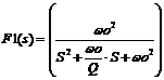
[given the response function]
Syed M. Ahmed
The system requirements for a Notch Filter were defined by a third order Filter Transfer Function T(s) below. The required suppression of the undesired frequency was >40dB, with a short flat response around the Notch Center frequency instead of a narrow (indeterminate) dip; so that the Phase Shift of signal above and below the center was not appreciable.
The Transfer function by inspection can be broken down into Low-Pass F1(s) second-order, and High-Pass first-order F2(s) constituents.
![]()
Second Order LP Function
First Order HP Function
The Notch Filter is eventually realized by subtracting the selected (band-passed) range of unwanted frequencies from the incoming signal, as shown below. The factor ‘K’ represents scaling.
![]()
The above method of implementing the Notch (or Band-Stop) function is physically realizable, compared with the direct but not realizable approach, where a Low-Pass filter is cascaded with a High-Pass filter. In which case the low-pass segment must precede in order to permit the low frequencies to propagate. However, the Low-Pass filter would not allow the higher frequency response to build back up.
Conversely, in the implementation below the band-pass function is realized by reversing the high-pass low-pass order in the cascade. The high-pass break point is set at the start of the composite band-pass, followed by the low-pass filter cutting off the higher frequencies. The composite band-pass frequencies are then subtracted from the incoming band of signal frequencies to give the notched output.
Filter Design:
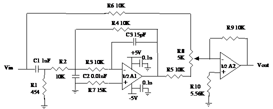
The composite notch-filter in Fig:1 below, comprises of a multiple-feedback topology second-order low-pass filter (--middle part of the circuit); preceded by a cascaded first-order high-pass section at the input. The combined low-pass high-pass filters constitute a band-pass filter with an inverted output. The notch function is realized by adding the direct signal (--over R6) to the inverted band-pass component (--output driving R5) to produce an inverted notch. The second stage simply inverts the signal back and scales it. The potentiometer at the input allows fine tuning the notch depth by choosing the exact proportion of direct signal with the inverted band-pass signal from the filter output.
Starting with the second-order low-pass function first; the filter can be synthesized in any number of ways such as Butterworth, Chebyschev or Thomson type. While hardware configuration could be Sallen-Key or Multiple Feedback depending on the various desired attributes. Since the filter transfer function was provided along with coefficients and preference for minimal (well behaved) phase around the notch center. The design was chosen to be the middle-path between Butterworth and Chebyschev functions; or the Transitional Filters class. The Transitional domain in its middle portion displays a fairly linear-phase response and low ripple, depending upon the location of the poles. Further, the circuit topology was chosen to be multiple-feedback as it requires fewer components (Op-Amps) and delivers better out-of-band performance.
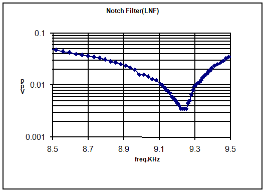
Third-Order Notch Filter:
Fig:2 below shows the response of the above Notch Filter --note the 'flat' around the center.
Sensitivity:
The center frequency f0 sensitivity to tolerance in resistor and capacitor component values is given by:

Resistor Sensitivity Capacitor Sensitivity
Since the center frequency is determined by R1-3 and C1-3, therefore

![]()
It can be shown that
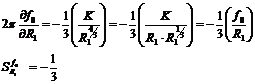
Likewise for other R and C

The design was implemented with 1% resistors and 10% capacitors, yielding the higher figure for capacitors
![]()
which translates to ~3.33% change in f0 due to 10% change in capacitor values; corresponding change of 0.33% due to resistors changing through 1%. Since the center frequency f0 by original requirement was 10KHz the overall change in f0 comes to 333Hz and 33.3Hz for capacitor and resistor variations. The component values in the schematic are for the tweaked f0 slightly off-center corresponding to the pre-production models of the sensors in the first prototype.
Reference:
Passive and Active Network Analysis and Synthesis by Aram Budak, Houghton Mifflin Company, 1974. ISBN: 0-395-17203-9